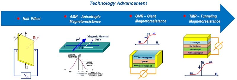
Magnetic transducers are widely used in modern industry and electronics to sense the magnetic field strength to measure current, position, motion, direction, and other physical parameters. In the technical field of magnetoresistive transducers, there are many different types of sensors for measuring magnetic field and other parameters. Commercially important ones, in order of technical advancement, include: Hall Effect, Anisotropic MagnetoResistance (AMR), Giant MagnetoResistance (GMR), and the latest:Tunneling MagnetoResistance (TMR).
The Hall element is a magnetic sensor sensing element for which the applied magnetic field is typically amplified using magnetic flux concentrator to improve the sensitivity of the Hall output, thereby increasing the size and weight of the sensor. Hall elements have large power consumption and poor non-linearity. The AMR element has much higher sensitivity than the Hall element, but it has a narrow linear operating range. The AMR magnetic sensor sensing elements need to use a set / reset coil for their preset / reset operation. This results in increasing the complexity of their manufacturing process, while also increasing their size and power consumption. The GMR magnetic sensing element sensitivity is higher than for AMR, but its linear range is still low.
Recently, TMR (Tunnel MagnetoResistance) elements were introduced as a new type of magnetoresistance sensor for industrial applications. They are constructed as a magnetic multilayer film material. TMR magnetic field sensing elements exhibit a greater change in resistivity, as a function of applied magnetic field induction, than that of the previously developed magnetoresistance technologies, AMR and GMR. The term Magnetic Tunnel Junction (MTJ) is used to refer to a TMR sensing element.
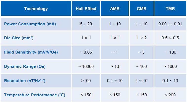
Relative to a Hall effect element, an MTJ element has better temperature stability, higher sensitivity, lower power consumption, better linearity, and needs no additional flux concentrator structure. Relative to an AMR element, an MTJ element has better temperature stability, higher sensitivity, wider linear range, and needs no set / reset coil. Relative to a GMR sensing element, an MTJ has better temperature stability, higher sensitivity, lower power consumption, and a wider linear range.

Figure 1: Schematics of four generations of magnetic sensing technology
In Table 1, the technical performance parameters of a Hall element, AMR element, GMR element and TMR element, are contrasted. One can more clearly see the pros and cons of the various technologies:
Table 1: Comparison of Magnetic Sensing Technology Parameters


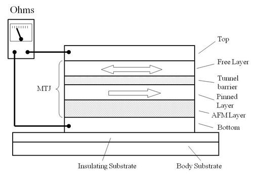
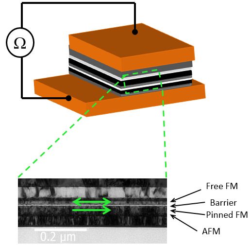
Figure 2: MTJ element cross section diagram Figure 3: MTJ element TEM image
Figure 2 is a schematic cross section diagram of the MTJ element structure. The three main layers in an MTJ element are, from bottom to top: a pinned ferromagnetic layer, the tunnel barrier layer, and a free ferromagnetic layer. The bottom ferromagnetic layer is a composite layer formed of an anti-ferromagnetic pinning layer and a ferromagnetic layer. Antiferromagnetic exchange coupling between the pinning layer and the pinned layer strongly couples the magnetic behavior of those two layers together. The tunnel barrier layer is generally made of MgO or Al2O3. The top ferromagnetic layer is “free” because there is no “pinning layer”as there is on the bottom. The large arrows represent the directions of the pinned layer and free layer magnetizations. The pinned layer magnetization direction is relatively fixed in the presence of modest magnetic fields. The free layer magnetization direction is relatively easy to rotate in small to modest magnetic fields. The typical thickness of each layer is between 0.1 nm to 100 nm.
Figure 3 is an MTJ element (Transmission Electron Microscope, TEM)image.
The Bottom Conducting Layer and the Top Conducting Layer are in direct electrical contact with the antiferromagnetic layer, and the free layer, respectively. The electrode layers are usually a non-magnetic conductive material. These layers form electrodes that carry input current from an ohmmeter through the tunnel junction, and connect to meters that measure the current (or voltage).Typically, the tunnel barrier layer provides most of the resistance of the device. The MTJ is about 1000 ohms, and the resistance of the remaining conductors is about 10 ohms. The bottom electrode layer is supported by an Insulating Layer. The Body Substrate is wider than the bottom electrode layer, and is located beneath all of the other layers. The Body Substrate material is usually silicon, quartz, heat-resistant glass, GaAs, AlTiC; or the wafer can be integrated with any other material. Silicon is often the best choice because of the ease of processing silicon integrated circuits (though integrated magnetic sensor circuits are not always required).

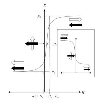
Figure 4: MTJ typical response curve
Figure 4 shows a typical response curve of Resistance R (Ohms) vs. Applied Magnetic Field H (Oersted).
In the ideal case, the response curve of Magnetoresistance (R) vs. Magnetic Field (H) is perfectly linear, and without magnetic hysteresis. (In reality, the R vs. H curve exhibits a hysteretic phenomenon called magnetic hysteresis. In actual recorded Magnetoresistance response curve loops, the hysteresis can be very small. For simplicity, the curve can be thought of being perfectly linear. In applications of real magnetic sensors, the magnetic sensor design constraints and defects in the material may cause this curve to be more irregular. The company has sensor designs, structures and manufacturing processes to produce this product with high quality in commercial quantities. These sensors have excellent working dynamic range, with high linearity, low hysteresis, and high sensitivity characteristics (i.e., a large magnetoresistive response curve slope).
The R vs. H curve has low and high resistance states,RLand RH, respectively. The high sensitivity portion of the curve is in the zero-field region, the sensor response saturates at about 1/3 of the maximum value on the plot. The slope of the response curve is proportional to the sensitivity of the sensor. As shown in Figure 4, the zero field tangent and low-field and high-field tangents intersect at tangent field values (-Hs + Ho) and (Hs + Ho); where Hs and Ho are abbreviations for the Saturation Field and Offset Field. One can see that the response curve is not symmetrical about the H = 0 axis. Ho is a typical bias field. The offset fields, Ho, are often called “Orange-peel Coupling" or "Néel Coupling", the typical values are 1 to 40 Oe. The coupling is related to the roughness of the magnetoresistive element’s ferromagnetic thin film structure, and is highly dependent upon the manufacturing materials and processes. Hs is quantitatively defined as the field at which the tangents of the linear region intersect with the tangents of the positive and negative saturation regions of the curve; all after the effect of the asymmetry H­o is removed. The white arrows represent the direction of the free layer magnetization. The black arrows represent the direction of the pinned ferromagnetic layer magnetization.
The magnetoresistance response curve shows the resistance change as a function of the angle between the magnetization directions of the free layer and the pinned layer. When the free layer magnetization is antiparallel to the pinned layer magnetization, the resistance has a maximum value RHigh (RH). When the free layer magnetization is parallel to the pinned layer magnetization, the resistance has a minimum value RLow (RL). When the magnetizations are at a perpendicular angle, the resistance is at a value halfway between RH and RL. This is often an ideal angle and field for the “operating point”of a sensor because of the linear behavior at that point.
In the right half of Figure 4, the small inset shows the R vs. H response curve for a sensor that has been rotated 180° about the axis normal to the sensing plane. In a field H applied along the sensing axis, these slope of the response curves of these two sensors are opposite one another. The main graph shows the R vs. H response for a sensor that has been rotated 0°. These two resistor types can be combined together to form a resistance bridge, which is a common way to compare the value of two different resistors.
A resistance bridge is often employed in a circuit application to change the magnetoresistance sensor electronic signal, so that its output voltage is easy to amplify. This can also reduce common-mode signals, provide noise cancellation, reduce temperature drift, and minimize other transducer deficiencies. The MTJ elements can be connected in parallel and/or in series to form a Wheatstone bridge or any other type of electronic bridge.

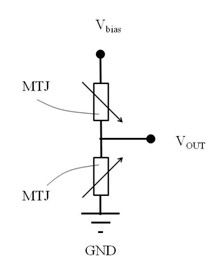
Figure 5: Push-pull half-bridge sensor block diagram
Figure 5 shows a typical half-bridge push-pull MTJ sensor construction. The sense axis of one MTJ magnetoresistor is rotated to be 180 ° from the other to form a half-bridge, which has three external contact pads, as follows: bias voltage (Vbias), center VOUT and ground (GND). The bridge circuit can be electrically connected through the pads, and a steady voltage Vbias is applied between Vbias and GND. For a given value of externally applied field, H, along the positive sense axis, the resistance increases for one resistor and decreases for the other. When the external field is applied in the opposite direction (along the negative sense axis) the resistance decreases for one while increasing for the other. These two magnetic field measurements have the opposite sign effect on the output voltage response – one resistance increases while the other decreases. This configuration can increase the sensitivity of the sensor, and is called a "push-pull" bridge circuit.
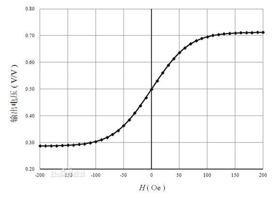
The half-bridge push-pull output voltage of the sensor can be measured using many typical methods. For example, a voltmeter is connected between VOUT and GND, and the VOUT and GND potential difference (V VOUT-GND) is the output voltage. A typical analog output curve is shown in Figure 6.

Figure 6: Push-pull half-bridge sensor output curve simulation results
The MTJ bridge output curve is an analog voltage signal. One can design a circuit system containing a dedicated ASIC chip, analog signal processing, and digital signal output, to meet the special requirements of a given application.
The discoverers of the GMR effect, French scientist Albert Fert and German scientist Peter Andreas Grünberg were awarded the 2007 Nobel Prize in Physics. A key reason cited is the tremendous contribution to the technical fields of modern magnetic recording and industrial magnetic sensors. TMR is the next generation of magnetoresistance technology to follow after GMR. TMR (MTJ) elements have completely replaced GMR elements in the hard disk drive read head application. One can expect that TMR magnetic sensor technology will take over other industrial applications as well, such as: bio-sensing, Magnetic Random Access Memory (MRAM), and other areas of great technical advancement and societal contribution.


